
Transistors (and their offsprings) are a fundamental part of every electronic device: our transistor biasing calculator will help you discover and understand how they work and how minor circuit modifications lead to noticeable differences in the operations of those small, ubiquitous components.
Keep reading for a full immersion in the world of our small, three-legged friends. Here you will learn:
- What are transistors, and how are they made?
- What are bipolar junction transistors (BJT)?
- The two types of BJT transistors.
- How does a transistor work?
- What is transistor biasing?
- The most important biasing techniques.
What are transistors?
A transistor is an active electronic component based on semiconductors. Transistors are mainly used as switches or amplifiers (you can discover one of their applications at our op-amp gain calculator). How so?
Get ready because, in a single sentence, we will unveil the transistors' secret: in such a device, a current flowing between two terminals can be controlled by a smaller (way smaller) current flowing in the device from a third terminal.
Let this sink in, and then keep reading to truly understand what is going on with terminals and currents.
🙋 Our transistor biasing calculator deals only with bipolar junction transistors (BJT). You will later understand why we call them so: only remember that we will use "transistor" and "bipolar junction transistor" interchangeably.
First, let's identify the components of a transistor. A bipolar junction transistor connects to the outside world through three terminals:
- The collector;
- The emitter; and
- The base.
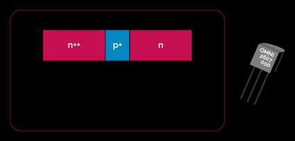
Each terminal leads to a semiconductor bulk (usually pure silicon) that underwent doping.
If you are an athlete, doping is a terrible thing. However, if you work in the semiconductor industry, doping is a good thing. If you are both, it depends.
A doped semiconductor is a semiconductor in which the introduction of defects led to the emergence of a particular kind of majority charge carrier. There are two types of doped semiconductors:
- p-type semiconductors, where the majority carriers are positively charged holes; and
- n-type semiconductors, where the majority carriers are negatively charged electrons.
Semiconductors are dope: the possibility of tuning the charge carriers produces important effects that are at the base of the functioning of the transistor.
If you pair a bulk p-type semiconductor and an n-type one, you create a so-called p-n junction, one of the pillars of modern electronics. In a p-n junction, an electrical current can flow only in a specific direction (you can see this behavior in diodes). A transistor is nothing but two paired p-n junctions.
🔎 Diodes are a fundamental component of electronics: you can find them (almost) everywhere. You can find out more here at Omni Calculator, from the basics with our Shockley diode calculator to more advanced topics with our the LED resistor calculator or our bridge rectifier calculator!
We know you raised an eyebrow here, and you are right: you can pair the junctions in different ways. There are two types of bipolar junction transistors:
- NPN transistors, where the majority charge carriers are electrons; and
- PNP transistors, where positive holes are the majority carriers.
🙋 In the transistor biasing calculator, we will consider only the NPN transistor: since electrons are the best type of charge carriers, they work better than their PNP counterparts. Luckily, the operations of a PNP transistor are identical to the NPN's one: you only have to invert the signs and the polarities.
Two similar symbols correspond to the two types of transistors. In both of them, an arrow marks the direction of the majority charge carrier. It is fundamental to learn the difference since a PNP transistor in place of an NPN transistor would not work — at best! At worst, you would have one transistor fewer than before. 😉

Each terminal of the two junctions corresponds to an element of the transistor. In the NPN type, we have:
- The emitter corresponds to an n-type semiconductor. Since it emits the charge carriers, it needs to be heavily doped.
- The base corresponds to the p-type semiconductor in the center. It is slightly less doped than the emitter.
- The collector, lightly doped, corresponds to the second n-type terminal.
So, how does a transistor work?
A transistor's working day
A transistor, as said, works by controlling a bigger current (or voltage) by employing a smaller current (or voltage).
To understand the operations of an NPN transistor, follow the diagram below. We apply a voltage to the base-emitter junction. In this case, the polarity respects the preferred direction of the junction (forward bias), and we witness a current flowing from the base to the emitter.
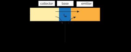
At this stage, the fabrication of a transistor becomes relevant: the base terminal must be thin enough to allow the charge carriers to reach the other p-n junction. If the p-doped layer, rich in holes, is too thick, the electrons coming from the emitter would recombine with the holes.
The collector-base junction is in a regime of reversed bias that makes the current flowing between those two terminals negligible.
And here the final magic of the transistor comes: since the collector is more lightly doped than the emitter, the electrons can easily cross the junction (if the electric field in the depletion zone is convenient for them), thus creating, effectively, a strong emitter-collector current.
The emitter-collector current is much bigger than the emitter-base one: their ratio defines one of the most important parameters of a transistor: the gain:
🙋 Every transistor has its specific value of , depending on the fabrication process. To correctly operate your device, that's a piece of information you need to know! How to discover it? You can measure it.
What is a transistor Q-point?
A transistor can operate in many "modes". Those modes lie on the load line, a line drawn on the collector current - collector-emitter voltage, between the two "extreme" modes:
- Saturation, where the voltage drop across emitter and collector is null, and the transistor effectively acts as a short-circuit; and
- Cut-off, where the transistor behaves as an open circuit ().
Along the load line, in a position dependent on the function of the transistor, lies the Q-point (from quiescent), the set of values for which the device is stable if no signal (as an AC current) is applied.
The correct choice of the Q-point allows the device to avoid entering the saturation and cut-off mode during operations — unless that's the very purpose!
How to operate your NPN transistor: transistor biasing
Now that you know how a transistor works, let's learn how to use it in some circuits: that's where calculations get practical — and interesting.
Biasing, in electronics, is the definition of the initial conditions in which an active component operates. You can bias a transistor in many possible ways. Here we will learn the most common ones.
First, let's draw a circuit with a transistor and identify the main elements here too.

On the side of the collector, we identify a voltage source we call . Its counterpart (though not always it will appear in the circuits) on the emitter side is .
The voltage drops between the terminal of the transistor and the ground are identified with single letters: we then have , , and . Be careful: may identify both the voltage drop on the base and the bias to the terminal from time to time.
In this case, comes from the presence of a resistor, , between the voltage source and the transistor. In this diagram, and both equal .
Talking about currents, the most important ones are , the current flowing through the base, and , the collector current. , the current flowing through the emitter, is usually almost equal to .
Something else? Yes. You can identify voltage drops across two terminals of each junction. Their values are fundamental for the operations of the transistor. You then have , , and .
In a silicon transistor, the value of the voltage drop between the emitter and the basis (the forward-biased junction) is almost fixed and depends on the physics of the device. In our calculations, it will have a default value of .
Explaining why it has this value is out of the scope of our transistor biasing calculator!
Transistor biasing methods: fixed base bias biasing
The first configuration we explore is the simplest one, the fixed base bias. As the name suggests, the bias (voltage drop) on the base, , remains constant during the operations of the transistor. The relative circuit shows how to obtain this set-up:

In the circuit above depends on the value of , but you can also feed it with an independent constant voltage source (). Choose carefully the value of , the base resistance, to set the adequate bias.
Let's start exploring how a fixed base biased transistor operates. Apply the Kirkhoff's voltage law to the base-collector loop, and we find:
We can calculate the collector current using the value of the gain :
We can define a flurry of other quantities in this configuration:
Remember that the value of depends on the transistor type: for silicon, it is .
The fixed base biasing technique has many downsides, mainly a high dependence on the value of due to the bias imposed by the base current. Thermal effects also negatively affect the operation of a transistor in this configuration. However, it remains the easiest biasing method to understand. Let's move to something more advanced!
Transistor biasing methods: feedback biasing
The operations of a transistor can be stabilized by using feedback from the other terminals of the device. We can identify two main types of feedback biasing:
- Collector feedback biasing; and
- Emitter feedback biasing.
Collector feedback biasing
In the fixed base biasing, the transistor can find itself outside its active region since there is no control over the Q-point: nothing counteracts oscillations in the base or collector currents. However, suppose you connect the base terminal to the collector. In that case, you provide the base bias voltage as a function of the collector voltage , giving added stability to the biasing. Let's see how!

In this configuration, a drop in voltage on the collector, following, for example, an increase in , causes a corresponding reduction of the base voltage and a decrease in , which in turn lowers the collector current thanks to the relationship : the transistor is Q-fixed.
Take a look at the equations governing the behavior of a collector feedback-biased transistor. They are slightly different than the one we saw previously!
Look at the second expression containing . There lies the dependence of on the collector voltage, which allows for the feedback mechanism.
Here too, we can define the remaining equations:
Remember, as usual, that .
Emitter feedback biasing
The second feedback biasing configuration we consider adds another resistor, this time right after the emitter: . The rest of the circuit comes straight from the fixed base biasing one. Here is the circuit:

The presence of causes a voltage drop to develop at the emitter terminal. By applying the Kirkhoff's voltage law, we count all of the voltages in the base-emitter loop:
As you can see, the current now depends on the current . A variation in the latter causes the former to change in the direction that counteracts the variation, thus creating feedback against variation in .
Let's check the remaining formulas:
On the downside, a variation in the collector current has no feedback and can cause uncontrolled variations in the output due to a change in the value of .
Luckily, another biasing technique addresses most of the issues of the previous ones: the voltage divider bias.
Transistor biasing methods: voltage divider bias
We now introduce a transistor's most common biasing technique, the voltage divider bias. Its name comes from the fact that the two base resistors create a voltage divider with output on the base terminal of the transistor.
🔎 We made an entire tool dedicated to voltage dividers: if you want to learn more about them, visit our voltage divider calculator.
Here you can see the relative circuit:

In the voltage divider configuration, we use again the fixed base biasing. The addition of the other resistor connected to the base terminal adds control to the biasing — acting effectively as a voltage divider.
The presence of the emitter resistance adds feedback against variations in , Q-fixing the transistor.
Let's explore the most important equations that model this biasing technique.
The voltage divider biasing is largely employed in circuitry, and it's often fundamental in amplification circuits.
How to use our BJT transistor biasing calculator
Our transistor biasing calculator offers you the possibility to calculate all the quantities in a transistor in four different biasing techniques:
- Fixed base biasing;
- Connector feedback biasing;
- Emitter feedback biasing; and
- Voltage divider biasing.
Choose the technique you need (we set voltage divider as default), and insert the known parameters of your transistor biasing circuit; our calculator will provide you the remaining values (but only if you give us enough material to work on!).
Biasing your transistor in numbers: a working example
Let's try our transistor biasing calculator with an example. Check you are in the voltage divider mode, and insert the following values:
For example, this is the configuration you usually find on Arduino boards.
Next, we set the resistors:
Some values will start to appear, but only the ones not, depending on the presence of the transistor. The final, and fundamental value we need to insert is the gain, . Let's set:
Now the calculator will be populated entirely; in particular, you'll see the currents finally assuming their values. What we see here is the transistor in operation.
Thanks to the equation for for a voltage divider bias:
We find that:
With the help of the gain, we can find the value of the collector current:
See that? That is how a transistor operates. Now try to simulate what would happen in case of a variation of the value of the gain, and discover the advantages of feedback on the bias current in the voltage divider bias.
A final word
Now you know how to bias a transistor and build any transistor biasing circuit. It's not an easy matter, and we are proud you made it to the end!
You can use this tool both in your homework (or studies) and in your experimentations, but remember: before connecting any element, first be sure to know how they work!
FAQs
What is the most common biasing technique for a transistor?
The most common biasing technique for a transistor is voltage divider biasing. In this technique, the transistor is inserted in a voltage dividing circuit, where the result of the partition corresponds to the voltage on the base terminal. The presence of a resistor on the emitter terminal adds feedback against variations of the gain ß.
How to bias a transistor using the fixed base biasing technique?
The core concept of the fixed base biasing technique is the presence of a constant voltage to the base terminal of the transistor. The current Ib flowing through the base and controlling the emitter current Ie does not change. Variations of the gain go unchecked. Other biasing techniques are usually preferred.
What is the value of the gain for a transistor?
The value of the gain ß of a transistor varies depending on the fabrication characteristics of the device itself. The exact value is not defined but lies in a range, with ß usually between 20 and 200. A typical (and ideal) value is 100.
The value of the gain also depends on the environment, being especially affected by thermal variations during the operations of the transistor. Biasing techniques that counter a variation of ß are usually preferred to one that left it unchecked.
How do I calculate the emitter current in a transistor?
To calculate the emitter current in a transistor:
- Multiply the gain of the transistor ß by the base current to get the collect current.
- Add the collector current to the base current.
- The result is the emitter current.
The determination of the values of the collector and base currents varies according to the biasing technique.
Discover more about this topic at the transistor biasing calculator at Omni Calculator!