Our MOSFET calculator will teach you everything you need to know about this ubiquitous electronic component, from the basics to the calculations of the MOSFET operations. Discover with Omni Calculator the component that, since the 60s, revolutionized the world.
Here you will learn:
- What are MOSFETs?
- What is the structure of a MOSFET?
- How does a MOSFET work?
- The operating regimes of a MOSFET.
- The triode and saturation MOSFET current equations.
- How to use our MOSFET calculator.
What are MOSFETs?
MOSFET stands for "metal-oxide-semiconductor field-effect transistor": a name that fills one's mouth for sure. Let's learn what it means.
- Metal-oxide-semiconductor is a reference to the structure of the device. We will shortly analyze these in detail.
- Field-effect transistor means that a MOSFET is a device able to control an electric current using an electric field (in contrast with other types of transistors, where the current is controlled by a smaller current).
🔎 The older bipolar junction transistors operate similarly to MOSFETs but with substantial differences. Learn more about them at our transistor biasing calculator.
As for other transistors, the MOSFET has three terminals:
- Source;
- Drain; and
- Gate.
In a few words, a change in the electric field on the gate electrode causes a variation in the electric conductance of a channel between source and drain.
Imposing a potential difference between source and drain, we can control the resulting current through a variation in , the gate voltage, until the device reaches a saturation state where it behaves, substantially, like a shorted circuit.
The structure of a MOSFET
MOSFETs rely on semiconductor technologies and a pinch of solid-state physics. The first element we meet is a semiconductor bulk called substrate. The substrate is lightly doped with impurities, which defines the type of MOSFET we are working on:
- p-doped substrate, used in n-type MOSFETs; and
- n-doped substrate, used for p-type MOSFETs.
In the substrate, we create two wells of doped semiconductor, either n+ or p+, depending on the type of MOSFET. The wells become the source and drain electrodes of the device. A stretch of semiconducting material called a channel separates the two terminals.
The surface of the semiconductor is oxidated, creating a layer of dielectric, which insulates the device. Above the channel, we can find a metal electrode (the gate), which we use to tune the electric field above the channel. The electrodes and the semiconductor make contact by employing openings in the oxide obtained through etching.
The gate is where we finally see the metal-oxide-semiconductor structure of a MOSFET!
In the diagram below, you can see the two types of MOSFETs:
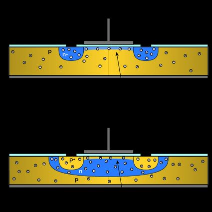
🙋 MOSFETs are symmetric. Reversing the polarity of the bias only reverses the direction of the current flowing in the device: this is opposite to the behavior of other types of transistors (such as the bipolar junction transistor), where the component can work only in a specified direction.
How does a MOSFET work?
Now that we know how a MOSFET is constructed, let's understand how it works.
There are two modes of operations of a MOSFET, depending on the level of doping of the substrate:
- Enhancement; and
- Depletion.
🔎 Visit our Shockley diode calculator to learn the most important application of doping in the semiconductor industry.
The names refer to the change in the state of the channel between source and drain. In enhancement-mode, the MOSFET is normally off: the channel lacks majority charge carriers, and the current can't flow between source and drain. Applying an opposite polarity than the one of the carriers to the gate electrode attracts carriers close to the gate itself, thus enhancing the conductivity of the channel. As a consequence, a source-drain current starts flowing.
The depletion-mode corresponds to the normally on state of the MOSFET. The channel is lightly doped, and a current is allowed to flow even in the absence of any gate voltage. This current is interrupted when the proper polarity (the same as the charge of the carriers) on the gate "pushes" the carriers away from the channel, in the direction of the substrate, thus depleting the channel and reducing its conductivity.
Depletion-mode MOSFETS are relatively uncommon. In our tool, we will focus only on the enhancement-mode MOSFET.
Let's consider an n-type MOSFET in enhancement mode. Usually, the channel connecting the two wells (source and drain) is lightly p-doped. However, the concentration of holes reduces if we increase the gate voltage . We can identify a characteristic value of called threshold voltage of a MOSFET, . When reached, an inversion layer forms between source and drain, with a concentration of electrons high enough for electrical conduction.
🙋 Don't worry: we created a tool specifically to help you calculate the threshold voltage of a MOSFET. Quick! Visit our MOSFET threshold voltage calculator! 😁
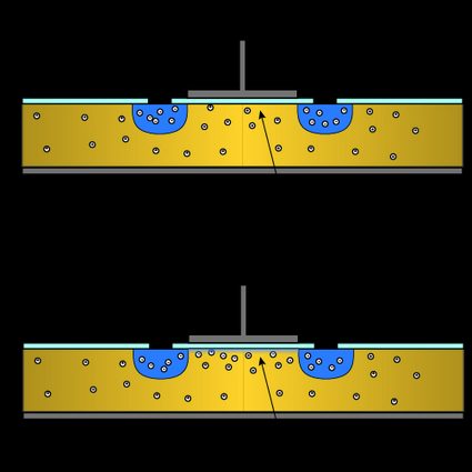
The structure of a MOSFET appears clearly in the symbols used in circuit design. In the image below, you can see the four possible types of MOSFETs.

The letters and mark the source and drain electrodes. The vertical line connecting them is the conductive channel, separated by a space from the gate electrode .
In the first row, the devices are in enhancement-mode. The line marking the channel is dashed — in the resting state, the channel is closed, and there's no passage of current. The symbols for the depletion-mode have a solid line as a channel: they conduct a current even in the absence of a gate voltage.
Column-wise we can find the other distinction of MOSFETs devices: the doping of the channel. You can see the n-type devices on the left, while on the right, there are the p-type devices. The difference lies in the direction of the arrow.
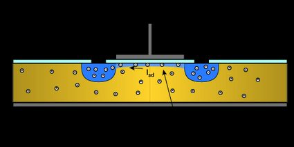
The regimes of operations of a MOSFET: saturation, triode, and cut-off
An n-type, enhancement-mode MOSFET has three distinct operating regimes, depending on the biasing of the device. Let's meet them.
Cut-off regime
In the cut-off regime, the gate voltage is smaller than the threshold voltage. There is a depletion region below the gate electrode but not an inversion in the concentration of charge carriers. This regime happens whenever the bias respects the following condition:
🙋 We used the gate-source voltage rather than the gate-body voltage since this is the most common choice in circuit design.
Theoretically, there is no current flowing between source and drain in this regime. However, thermal excitation and minority carriers can contribute to a small leakage current that is often negligible.
This regime corresponds to the off state of the MOSFET and is fundamental when the device is operated as a switch.
We pass the inversion by increasing the voltage past the threshold, and a current can flow across the device. The value of the source and drain voltages become relevant and help us define the other two regimes of operation of a MOSFET.
MOSFET triode or linear regime
To attain this regime, the biasing must satisfy these two conditions:
The source-drain current shows a strong dependence on the source-drain voltage, and follows an ohmic behavior with equation:
🔎 Here we can identify the geometric parameters of the channel:
- is the width of the channel; and
- its length.
Together, these two quantities define the W/L ratio. The other parameters are:
- – Mobility of electrons in the channel; and
- – Capacitance of the oxide layer.
The combination gate voltage and source-drain voltage defines a tilted line in the , typical for ohmic behaviors.
Saturation regime
In this regime, the source-drain voltage is high enough to widen the channel and provide an electric field high enough to "push" the charge carries (in the n-type MOSFET, electrons) across the channel even if the gate voltage is not high. The source-drain MOSFET saturation current equation is:
There are many similarities with the linear regime current equation; however, it's straightforward to see that we lost the dependence on the source-drain voltage, retaining only the one on the gate voltage.
The quantities used in the equations for the drain current are often grouped in a single constant called :
Which reduces the equations to:
You can compute the value of through the quantities reported on the datasheets, often in the electric characteristics data.
The three modes are easily identified on the current-voltage characteristic curve:
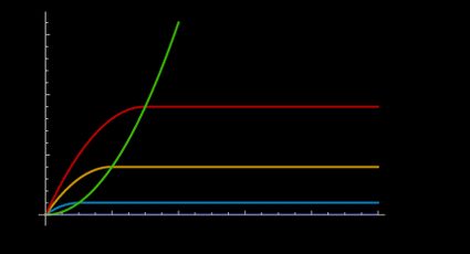
The current is null for any gate voltage below the threshold voltage: this corresponds to a line on the horizontal axis. Once the gate voltage passes the threshold, we enter the other regimes, starting with the MOSFET triode region.
You can distinguish the linear regime in the left part of the graph. For increasing gate voltages, the channel opens more, and the conducibility of the channel increases.
Once the source-drain voltage reaches a specific value, we enter the MOSFET saturation region, where the current stabilizes at a value dictated only by the gate tension. This part corresponds to the horizontal plateaus at increasing currents for increasing values of .
How to use our MOSFET calculator
To use our MOSFET calculator, you need to input the parameters of the current equations for the MOSFET.
The inputs you give to our MOSFET calculator will decide if you are in the cut-off, triode, or saturation region of the MOSFET.
To compute the current, you need to know the value of the parameter of your MOSFET and the threshold voltage. You can either measure it or search for the declared value on the datasheet.
If you expand the MOSFET Structure Parameters section of the tool, you will be able to insert the values of the parameters making up :
- Parameters of the MOSFET structure: width and length of the channel.
- Capacitance of the MOSFET's layer oxide.
- Electron mobility .
Let's take one of the most popular MOSFETs you can use in your circuits, the BS170. From the datasheet you can easily find the value of the typical threshold voltage, . We computed the value of extrapolating the values of and in saturation regime from the characteristic, and plugging them in the rearranged formula for the saturation current:
Knowing the value of and , we can compute the source-drain current in any regime. Imagine imposing a source-drain voltage and a gate-source voltage . This biasing puts us in the linear region, where we can calculate the current with:
Our journey with the MOSFET ends here. However, we created other tools that can help you in your discovery of electronics. Try our logic gate calculator to learn the most basic application of MOSFETs, or our crosstalk calculator to discover the limitation of integrations in computer processors.
FAQs
What are the MOSFET operating regimes?
The three MOSFET operating regimes are:
- Cut-off, when
Vgs < Vt: the device is turned off. - Triode (or linear), when
Vgs ≥ VTandVds ≤ Vgs - VT: the device operates as a variable resistor. - Saturation, when
Vgs ≥ VTandVds > Vgs - VT: the drain current flattens at a value decided by the gate voltage.
Discover more about them and how to calculate the current in a MOSFET at Omni Calculator.
Why does the current of a MOSFET saturate?
Upon reaching a value of source-drain voltage higher than the difference between the gate and the threshold voltage (Vds > Vgs - VT), the tension "pinch" the channel in the proximity of the drain electrode, effectively removing the dependence of the current on Vds. The saturation region in a MOSFET corresponds to the fully turned-on mode of the device.
What is the saturation current of a BSS138 MOSFET when the gate tension is 10 V?
The saturation current is 41.9 A. Taking the parameters from the datasheet, we know that:
- Threshold voltage is
VT = 1.3 V; and - K parameter is
K = 0.5536.
Plug the values in the equation for the saturation regime current:
ID = K × (Vgs -VT)² = 0.5536 × (10 - 1.3)² = 41.9 A
The BSS138 is known for its performance at low voltages and high currents.
What is the current of a MOSFET in the triode region?
In the triode (or linear) regime, the drain current of a MOSFET is:
ID = (W/L) × Cox × µN × (Vgs - (Vds/2) - VT) × Vds
where:
W/L– Width to length ratio of the MOSFET's channel;Cox– Capacitance of the oxide layer;µN– Electron mobility;Vgs– Gate voltage relative to the source;VT– Threshold voltage; andVds– Source-drain voltage.