MOSFET Threshold Voltage Calculator
- What is a MOSFET? – a quick explanation
- The types of MOSFETs
- Operations of a MOSFET
- What is the MOSFET threshold voltage?
- The regimes of operations of a MOSFET device: above (or below) the threshold voltage
- How to calculate the threshold voltage of a MOSFET
- The body effect in MOSFETs
- How to use our MOSFET threshold voltage calculator
- What about depletion-mode?
- FAQ
Our MOSFET threshold voltage calculator will help you understand the principles of operation of the most important electronic device ever conceived. If you've ever asked yourself, "how does my computer work?", then this tool is a great starter!
Here you will find:
- A quick introduction to MOSFETs.
- What is the threshold voltage of a MOSFET?
- How the regimes of operation depend on the MOSFET's threshold voltage.
- How to calculate the threshold voltage of a MOSFET.
- What is the body effect in a MOSFET?
And much more.
What is a MOSFET? – a quick explanation
A MOSFET is a semiconductor-based device that works similarly to a transistor. The expansion of this acronym suggests this similarity: metal-oxide-semiconductor field-effect transistor. We explain in detail what this means in our MOSFET calculator!
As for the transistor, in a MOSFET, we act on a control parameter to tune a large current flowing across two electrodes. We talked in detail about "traditional" transistors in our transistor biasing calculator.
A technical overview of MOSFETs
MOSFETS are conceptually easy to understand, but as it often happens, their potentialities only hide behind this lack of complexity.
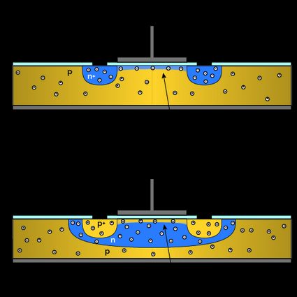
A large bulk-type semiconductor called the substrate hosts the devices. In the substrate, using a process of diffusion, two wells with opposite doping originate the source and drain electrodes. The electrical current flowing through the device will pass through both of them.
Between source and drain, we identify a region called the channel. The channel lies directly underneath an oxide layer (usually obtained through oxidation of the semiconductor or deposition) and a metal terminal (the gate), thus originating the metal-oxide-semiconductor structure.
The types of MOSFETs
According to the doping of the MOSFET, we can identify two main types of devices:
- n-type MOSFETs, also known as n-channel MOSFET; and
- p-type MOSFETs, also known as p-channel MOSFET.
The substrate of an n-type MOSFET is doped with electron acceptors (p-type). The source and drain wells are n-doped, while the channel connecting them presents an excess of holes. The description is the opposite for a p-type MOSFET.
Another distinction is possible. If we slightly change the doping of the channel, the presence of charge carriers changes its electrical conductivity. In a "rest" condition (where the gate voltage is null), we can identify two possible types of MOSFET:
- Enhancement mode MOSFETs, which are usually off and don't conduct electric currents; and
- Depletion mode MOSFETS in which a current flows when the gate voltage is 0, thus being typically on.
Operations of a MOSFET
To analyze the operations of a MOSFET, we will focus on n-channel devices. The description is similar for the p-type MOSFETs, only requiring some straightforward modifications (the majority of charge carriers being holes instead of electrons).
🙋 If not specified, our MOSFET threshold voltage calculator uses interchangeably "MOSFET " and "n-type MOSFET". When not explicitly stated, assume we are talking of an n-type device.
A MOSFET in depletion-mode conduces a current even when the gate voltage is null (). An adequate negative voltage to the gate electrode pushes the electrons away from the channel, effectively closing it.
In enhancement-mode, the channel is normally devoid of majority charge carriers (in the n-type MOSFET, electrons). A positive voltage on the gate electrode attracts them to the interface of the insulator layer, thus progressively opening a conductive channel between source and drain.

In both modes, before we manage to change the behavior of the MOSFET, we need to reach a value of gate voltage called threshold voltage.
What is the MOSFET threshold voltage?
The threshold voltage controls the operations of a MOSFET device by marking its different states (on and off). The interplay of the other control parameters of the devices originates the different modes of operations of a MOSFET.
The threshold voltage is characteristic for the device, depending on both environmental and fabrication parameters, and it works as a separation between different operating regimes of the device.
The threshold voltage is the minimum voltage capable of opening a conductive channel between source and drain. Physically, this condition is required because the semiconductor outside of the wells is p-doped. An excess of positive charges (holes) must be balanced before free electrons can eventually become majority charge carriers.
We identify two main situations depending on the value of the threshold voltage:
- Depletion; and
- Inversion.
During the depletion phase, the gate voltage increases, and the charge carriers (holes) in the area of the channel recombine with the oppositely charged ones (electrons) attracted by the gate. At one point, the channel contains no free charge carriers. Increasing the gate threshold further can attract charge carriers in the channel, concording in sign with the MOSFET wells.
These carriers are the ones responsible for the current between source and drain. Since we effectively changed the semiconductor doping, we call this situation inversion. We reach the threshold voltage when the charge carriers concentration in the channel equals the one in the bulk.
Remaining in the context of n-type MOSFETs, we can study how the device's behavior depends on the value of the threshold voltage and the source-drain voltage.
The regimes of operations of a MOSFET device: above (or below) the threshold voltage
Varying the gate, source, and drain voltage allows using a MOSFET device in three different modes. Let's check them out.
🙋 We will analyze the three regimes for an enhancement-mode n-channel MOSFET, as depletion-type devices are relatively uncommon. Their description is, however, not much different!
Cut-off mode
When the source-gate voltage is lower than the threshold voltage:
The channel remains closed, with the gate potential not strong enough to attract charge carriers between source and drain. A small current is still allowed to flow but is often negligible. This regime is attained in any condition of source and drain voltages.
Triode mode (linear region)
This regime finally sees the gate voltage higher than the threshold voltage. The complete configuration of this regime sees these two inequalities satisfied:
...where is the voltage drop between the source and the drain. In this region, the channel is open and allows the passage of an electric current. The behavior of the device is resistive. If we increase the source-drain tension, the source-drain current increases following a slanted like according to Ohm's law.
Saturation (active mode)
When the source-drain voltage reaches a certain level, the source-drain current saturates.
The I-V curve clearly shows the behavior of the MOSFET. We talked in-depth about these topics in the MOSFET calculator.
The MOSFET's ability to switch from a completely-off (cut-off) state to a completely-on state (saturation) made them the ideal choice for building the logic gates at the base of the operations of a logic processor. Discover more about the topic at our logic gate calculator!
How to calculate the threshold voltage of a MOSFET
The value of the threshold voltage of a MOSFET depends, at first glance, on the fabrication parameters of the device itself. The formula used to calculate the threshold voltage is:
where:
- – Permittivity of silicon;
- – Elementary charge;
- – Doping concentration of the substrate;
- – Capacitance of the oxide between substrate and gate electrode per unit of area; and
- – Surface potential for inversion.
🔎 The capacitance of the oxide layer is a crucial parameter in the design of a MOSFET: too high, and the device will be insensitive to change in gate voltage; too low, and the device would switch for minimal interferences.
We need to talk a bit about . The surface potential is the potential between the bulk of the MOSFET and the surface of the channel. We call it . If undisturbed, the surface potential value depends on the MOSFET's doping. We need to reach a surface potential twice as big as the initial one to achieve inversion. We define the potential for inversion as:
In this equation, we find some other parameters:
- Temperature ;
- Boltzmann's constant ; and
- Intrinsic carrier concentration in the semiconductor, .
We made an entire calculator to explain in detail what is the intrinsic carrier concentration. Visit our intrinsic carrier concentration calculator to learn more about the physics of semiconductors.
The body effect in MOSFETs
We can introduce a minor modification in the definition of the threshold voltage. The previous description assumes that the gate voltage is relative to the one of the substrate (or body). However, this is often not true: engineers prefer to connect the gate to the source.
Disjoining the gate and the body adds a dependence of the threshold voltage of a MOSFET on the substrate voltage: we call this effect the body effect of a MOSFET. The body effect is due to electrons' attraction (or repulsion) from the substrate electrode. Since the resulting effect is comparable (even if smaller in magnitude) to the action of the gate on the charge carriers, we can call the substrate a back gate.
The equation for the body effect of a MOSFET influence on the threshold voltage is:
where is the body effect coefficient, defined as:
...and is the body-source voltage. The presence of this voltage changes the behavior of the depletion zone, increasing the threshold voltage: the inversion is slightly harder to reach.
How to use our MOSFET threshold voltage calculator
Input all of the parameters you know in our MOSFET threshold voltage calculator, and we will give you the answer.
The result you get in the threshold voltage field is either , the threshold voltage relative to the body, or , the threshold voltage considering the body effect, depending on if you change the value of .
We moved the parameters changed less often (the charge of the carriers and the permittivity) to advanced mode. Click on the button to change their value. We use the relative permittivity in our calculator, related to the permittivity by , where is the vacuum permittivity.
Let's look at an example. Consider a typical MOSFET with the following values:
- Capacitance per unit area: ;
- Substrate dopant concentration: ; and
- Surface potential: .
Input these values in the calculator in the corresponding fields. We can fill the unknowns in the MOSFET threshold voltage equations:
The value is not far from the one you can meet in commonly used MOSFET devices.
What about depletion-mode?
A depletion-mode MOSFET is conceptually not much different from its regular MOSFET counterpart but has a much more complex description. Only a few clumsy models are available and are often used for simulations on software like SPICE.
If you measure the threshold voltage of such a MOSFET, however, the description of the regimes of operation of the device still holds. You only have to replace an increase in the number of majority charge carriers with a decrease in their concentration.
FAQ
What is the threshold voltage of a MOSFET?
The threshold voltage of a MOSFET is the gate voltage for which the device's channel has a charge carrier concentration equal to the one in the bulk. In an n-type MOSFET, when the gate voltage reaches the threshold voltage, the concentration of free electrons in the channel equals the concentration of holes in the bulk. When the value is attained, the channel can conduct an electric current.
How do I calculate the threshold voltage of a MOSFET?
To calculate the threshold voltage, gather the construction parameters of the MOSFET device:
- The capacitance of the oxide per unit of area C₀.
- The doping concentration of the substrate NA.
- The intrinsic concentration of charge carriers ni.
The expression for the threshold voltage is:
VT = √(2·Ɛ·q·NA·(2ΦF))/C₀ + 2ΦF
What is the body effect in a MOSFET?
The body effect in a MOSFET is a modification introduced to the threshold voltage to account for a gate voltage relative to the source electrode and not the device's substrate. In this situation, the substrate acts as a back gate, tuning the threshold voltage according to the MOSFET body effect equation:
VT = VT0 + γ(√(2ϕF + Vsb) - √(2ϕF))
where:
VT0– Threshold voltage relative to the substrate;γ– Body effect constant;ϕF– Surface potential for inversion; andVsb– Source-body voltage.
What is the typical value of the threshold voltage for an n-type MOSFET?
Between 0.7 V and 1 V. This is the typical value for the threshold voltage of a 5 V logic n-type enhancement-mode MOSFET. Any input voltage below this value will keep the MOSFET off, while any input higher than this will turn the MOSFET on. An invalid region around the threshold voltage avoids erratic behaviors by creating a sharp boundary between the two states.